
Daily Podcast full article
TSMC starts commercial 2nm production
TSMC has moved its 2-nanometer process from promise to commercial production, a milestone that matters less as a naming contest and more as a supply-chain test for AI, high-performance computing and premium electronics.
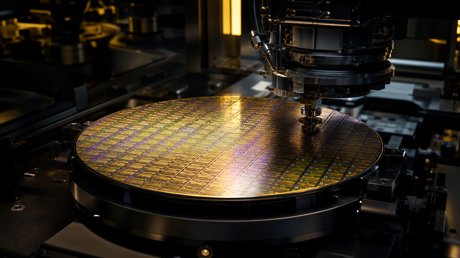
The headline: 2nm is now a manufacturing story
TSMC has begun commercial production of 2-nanometer chips, turning one of the semiconductor industry’s most closely watched roadmap items into a real production ramp . The shift matters because the most advanced process nodes are no longer just about making a faster phone chip or a denser server processor. They sit at the center of a global contest over AI infrastructure, power efficiency, fabrication capacity and the ability of chip designers to secure enough leading-edge supply.
The timing is notable. A fresh market note cited by Yahoo Finance says Bank of America expects the global semiconductor market to rise from about $1.7 trillion in 2026 to $3.2 trillion by 2030, almost doubling before the end of the decade . That forecast frames TSMC’s 2nm start not as an isolated technology event, but as a capacity signal: the foundry is preparing to feed a market where AI accelerators, data-center processors, memory systems and high-end consumer chips are all competing for advanced manufacturing slots.
Why 2nm matters beyond the label
The “2nm” name is not a literal measurement of one transistor feature in the simple way older process names once were. In modern chipmaking, node names are shorthand for a package of manufacturing improvements: transistor architecture, design rules, density, performance, leakage control, power management and yield learning. What matters commercially is whether a node gives customers a practical route to chips that run faster, consume less energy, or fit more logic into a given area.
That is why TSMC’s commercial start is important. The company is not merely announcing that it can make demonstration wafers; it is moving the process into commercial use . For customers, that changes the conversation from “when can we design for this?” to “how much capacity can we get, at what yield, and on what schedule?” For equipment suppliers, materials vendors and packaging partners, it changes the pressure as well. A 2nm ramp requires not just lithography tools, but steady process control, enough wafers, enough cleanroom capacity and enough downstream packaging for the chips that survive the front-end fab.
A separate Yahoo Finance item on TSMC described the move as part of a wider advanced-manufacturing push, with the company accelerating investment in cutting-edge fabrication capacity and raising capital-spending targets to support the 2nm rollout . That is the hidden center of this story: the milestone is technological, but the work ahead is industrial.
The supply-chain execution phase begins
Advanced nodes have always been expensive, but AI has made the economics even more demanding. The chips that train and run large models tend to be physically large, power hungry and dependent on advanced packaging. That means a 2nm wafer start is only the first step. The chip still has to be patterned, tested, diced, packaged, integrated with memory and delivered into systems that customers can deploy.
Recent reporting on TSMC’s capacity plans points to how fast the company is trying to scale. Digital Citizen reported that TSMC is preparing to lift monthly 2nm capacity from about 90,000 wafers at the end of 2026 to roughly 110,000 wafers by mid-2027, while 3nm capacity is expected to rise from about 180,000 to 210,000 wafers per month over the same period . If accurate, those figures suggest that 2nm will not be a boutique process reserved for a narrow set of showcase products. It is being prepared as a major production platform.
Still, “commercial production” does not mean instant abundance. Early capacity on a leading-edge node is usually allocated first to the largest and most strategically important customers. In practice, the first wave is likely to favor AI accelerators, high-performance computing chips and flagship mobile processors, because those products can justify the cost of the newest process technology. For smaller designers, the milestone may initially matter more as a roadmap anchor than as a near-term guarantee of supply.
AI demand changes the meaning of a node launch
The 2nm ramp lands in a market where demand is being pulled by AI infrastructure rather than by one consumer replacement cycle. Bank of America’s forecast of a semiconductor market growing toward $3.2 trillion by 2030 rests on continuing strength in AI infrastructure, memory and data-center demand . That matters because leading-edge nodes are increasingly tied to system-level economics. A faster or more efficient chip can lower energy costs, reduce cooling pressure, increase model throughput or let a cloud provider fit more compute into a fixed power envelope.
In earlier eras, the newest node was often framed around smartphones or PCs. Those categories still matter, but the center of gravity has shifted. AI clusters are power-constrained. Data centers are space-constrained. Cloud budgets are capital-intensive. In that environment, better performance per watt can be worth more than a simple peak-speed gain. TSMC’s 2nm process is therefore not just a chip story; it is also an electricity, cooling and infrastructure story.
That is why chip designers care so much about the timing. A company planning a next-generation AI accelerator or server CPU has to lock in design rules, packaging choices and manufacturing partners long before the finished product ships. Once a node enters commercial production, it gives customers more confidence to commit designs, place capacity reservations and coordinate with memory and substrate suppliers.
ASML, equipment and the bottleneck behind the bottleneck
TSMC’s latest 2nm reporting also highlights the role of ASML equipment in advanced manufacturing . At the leading edge, the foundry model depends on a dense ecosystem: lithography, etch, deposition, inspection, metrology, chemicals, gases, silicon wafers and cleanroom construction. ASML’s position in EUV lithography is especially important because the most advanced chips rely on extremely precise patterning steps.
That dependence cuts both ways. For TSMC, close alignment with equipment suppliers helps keep its technology roadmap moving. For the wider industry, it shows why advanced capacity cannot be added overnight. Even if demand is obvious, the tools are complex, costly and limited. A new 2nm fab is not simply a building with machines inside; it is a synchronized production system where one constraint can slow the entire ramp.
This is also why capital expenditure has become part of the node story. TSMC’s higher spending plans are not a footnote to 2nm; they are the mechanism that turns process leadership into deliverable wafers . Investors may focus on margins and returns, but customers are watching capacity, schedule credibility and yield improvement.
What changes for chip designers
For chip designers, the start of commercial 2nm production sharpens several decisions. First, they must decide which products deserve the newest node. Not every chip benefits enough to justify the cost. Control chips, connectivity silicon and many industrial components may remain on older, cheaper nodes for years. But AI accelerators, premium mobile systems-on-chip and high-end CPUs can gain meaningful advantages from a denser and more efficient process.
Second, designers must coordinate earlier with packaging. Modern high-performance chips often combine logic dies, high-bandwidth memory and other components in advanced packages. Digital Citizen noted that AI demand is putting pressure not only on wafer production but also on advanced packaging capacity such as CoWoS . In other words, a customer may secure 2nm wafers and still face a bottleneck if packaging capacity is tight.
Third, the launch forces competitors to respond. Other foundries can argue about timing, yields or alternative nodes, but TSMC’s commercial move sets a benchmark. Customers now have a real supply-chain reference point for 2nm-class production.
The milestone and the risk
The milestone is significant, but it does not remove execution risk. Early production must mature into stable yields. Capacity must scale without quality problems. Costs must come down enough for a wider set of products. Packaging has to keep pace. Customers must turn tape-outs into successful silicon. And the macro forecast behind the AI boom has to hold.
That is the realistic reading of the news: TSMC has crossed a line from roadmap to ramp. The next test is not whether 2nm exists, but whether it can be produced in enough volume, at enough quality, for enough customers to shape the next generation of electronics.
For now, Moore’s Law has not returned as a simple old rhythm. It has reappeared as a more complex industrial campaign: more capital, more equipment dependency, more packaging pressure and more AI-driven demand. TSMC’s 2nm start is the latest proof that the leading edge is still moving. The hard part now is making it move at commercial scale.
Sources from the last 72 hours
- [1]Taiwan Semiconductor Manufacturing (TSM) Starts Commercial 2 Nm ProductionSep 18, 2026, 12:00 AM UTC
- [2]BofA Sees Global Chip Market Nearly Doubling: Semiconductor ETFs to BuySep 18, 2026, 1:38 PM UTC
- [3]Why Is Taiwan Semiconductor Manufacturing (TSM) Ramping 2nm Production And Spending More?Sep 18, 2026, 10:12 AM UTC
- [4]TSMC Reportedly Targets 110,000 Monthly 2nm Wafers by Mid 2027Sep 16, 2026, 12:00 AM UTC
AI-generated article based on recent web research, then preserved as a dated editorial snapshot.
Comments
Be the first to comment.