
Daily Podcast full article
Tower plans $4B Japan chip hub
Tower Semiconductor is turning Japan into the core of its optical-chip manufacturing strategy, using a planned $4 billion program to expand silicon photonics, silicon germanium and advanced packaging capacity for AI-era data movement.
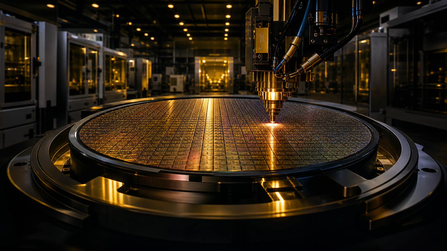
The new center of gravity
Tower Semiconductor’s Japan plan has moved from a broad investment pledge into a more concrete manufacturing map. In a Nikkei interview reported this week, CEO Russell Ellwanger said the Israeli foundry will make Japan its largest production hub for optical communications semiconductors as part of a planned $4 billion investment aimed at AI server demand . The update matters because it connects three separate trends that are now converging: Japan’s semiconductor revival, the foundry industry’s race to add specialized capacity, and the rise of optical interconnects as a constraint inside large AI systems.
The project is not just another fab headline. Tower is a specialty foundry, not a leading-edge logic giant, and its bet is focused on the chips and packaging technologies that help data move quickly between processors, memory, switches and accelerator clusters. Data Center Dynamics reported that the Japan program covers silicon photonics, silicon germanium and advanced packaging, and that the investment includes about $1 billion in support from Japan’s Ministry of Economy, Trade and Industry . CTech described the structure as roughly $3 billion of Tower investment backed by about $1 billion in Japanese government grants .
What Tower says it will build
The Japanese expansion is designed around existing sites and a new facility, rather than a single clean-sheet megafab. Tower plans to convert its Arai facility into a 300mm silicon photonics and advanced optical packaging site, while also increasing output at its Fab 7 facility in Uozu . A second step would add a new 300mm manufacturing facility next to the Uozu fab, giving the company a larger base for silicon photonics and silicon germanium capacity .
That sequencing is important. The first phase is expected to reach full production readiness in the fourth quarter of 2027, according to CTech . The new facility next to Fab 7 is expected to start making a significant financial contribution from 2029 . Data Center Dynamics, citing Nikkei Asia, reported a target of the equivalent of 45,000 300mm wafers per month in 2029, about 40 times the 2025 production figure, with around 200 additional workers to support the expansion . Private Infrastructure Daily framed the September update as adding site-by-site detail and a wafer target to a program whose headline capital plan had already been announced earlier .
Tower already has three manufacturing sites in Japan, alongside operations in Israel and the United States . That gives the company a base to expand from, and it helps explain why the Japan plan leans on conversion, capacity additions and local ecosystem building rather than only on a greenfield factory. AI Industry Today reported that the program spans Toyama and Niigata prefectures, with Arai in Niigata and Uozu in Toyama playing central roles .
Why optical chips matter for AI
The strategic logic is straightforward: AI systems are increasingly limited not only by how fast chips compute, but by how efficiently data can move among them. As accelerator clusters grow, electrical links face challenges in bandwidth density, heat and power. Silicon photonics uses optical signals to move data at high speeds, making it more attractive for links across racks, between switches and eventually closer to processors .
This is why Tower’s announcement reads as an AI infrastructure story even though it is not about GPUs. AI Industry Today wrote that demand is shifting semiconductor investment beyond compute chips toward the optical connectivity needed to link large accelerator clusters . CTech similarly noted that silicon photonics has become more important as data centers move enormous amounts of information between processors and other components .
The timing also follows signs of customer demand. Tower has contracts representing about $1.3 billion in silicon photonics revenue for 2027, and customers have already made about $290 million in prepayments to reserve capacity . AI Industry Today added that contracted wafer commitments for 2028 are even larger, according to the company . That does not remove execution risk, but it suggests the expansion is being built against visible demand rather than only a long-range market forecast.
A Japan industrial policy win
For Japan, Tower’s plan adds another anchor to the country’s semiconductor rebuilding strategy. The grant element places Tokyo directly inside a supply-chain layer that has become more important as AI hardware spreads beyond logic chips and memory. Private Infrastructure Daily put it plainly: the $1 billion state grant means Japan is effectively buying into one of the narrowest layers of the AI supply chain .
The project also extends Japan’s role beyond subsidies. AI Industry Today reported that Tower intends to develop a research and manufacturing ecosystem around Toyama and Niigata, including cooperation with suppliers, universities and research institutions . CTech also reported that Tower plans to expand cooperation with Japanese suppliers, universities and research institutions . That is consistent with Japan’s broader attempt to rebuild semiconductor depth across materials, equipment, packaging and specialty manufacturing rather than compete only at the most advanced logic node.
In practical terms, Japan gains a stronger position in optical connectivity, a category tied directly to AI data centers. Tower gains a manufacturing base in a country with semiconductor materials expertise, precision manufacturing culture and a government willing to share capital costs. The bargain is clear: public money helps de-risk capacity, while Tower brings demand signals and process technology.
The execution questions
The upside is large, but the plan is not automatic. Private Infrastructure Daily warned that a pledge is scheduled money rather than money already spent, and that the September interview added concrete site arithmetic without necessarily changing the capital commitment itself . The same report noted that Tower’s demand case is strong but that execution still depends on turning capacity, packaging and optical technology into customer-qualified output .
Several questions now matter. Can Tower convert Arai and expand Uozu on the 2027 timeline? Can it bring the new 300mm line to meaningful output by 2029? Can it scale co-packaged optics and related production technologies at the Uozu site, as Data Center Dynamics reported Ellwanger said Tower intends to do ? And can demand for AI optical interconnects keep pace with the capacity being planned?
The company’s financial targets show the ambition. CTech reported that Tower expects $3.6 billion in revenue and $1.2 billion in net profit in 2028, up from $1.6 billion in revenue and $220 million in net profit in 2025 . Those targets make the Japan project more than a regional expansion; they make it central to Tower’s next business model.
The takeaway
Tower’s $4 billion Japan chip hub is best understood as a bet on the next bottleneck in AI infrastructure. GPUs and memory still get most of the attention, but optical links are becoming the fast-travel system for data inside massive computing clusters. By concentrating silicon photonics, silicon germanium and advanced optical packaging in Japan, Tower is trying to secure a supply-chain position before the market fully matures.
For Japan, the project is another proof point that its semiconductor revival is not limited to national champions or headline logic fabs. For Tower, it is a high-conviction move into a market where speed, bandwidth and energy efficiency are becoming as strategic as transistor density. The photons now have a Japanese hub, and the race is to make it scale.
Sources from the last 72 hours
- [1]Israeli foundry Tower Semiconductor to make Japan main hub for optical chipsSep 24, 2026, 1:18 AM UTC
- [2]Tower Semiconductor to establish large-scale optical chip hub as part of $4bn Japanese investment pledgeSep 24, 2026, 12:00 AM UTC
- [3]Tower puts Japan at the center of its optical-chip strategySep 24, 2026, 7:30 AM UTC
- [4]Tower Semiconductor to Make Japan Its Largest Optical Chip Production HubSep 24, 2026, 5:30 AM UTC
- [5]Japan buys a quarter of Tower's $4bn optical chip betSep 24, 2026, 3:22 PM UTC
AI-generated article based on recent web research, then preserved as a dated editorial snapshot.
Comments
Be the first to comment.