
Daily Podcast full article
Applied Materials opens $5B lab
Applied Materials has opened its EPIC Center in Sunnyvale, a $5 billion semiconductor R&D facility built to bring chipmakers, tool engineers, systems companies and university researchers into the same development loop. The bet is that the next phase of Moore’s Law will be won less by building another fab than by shortening the lab-to-fab path for materials, packaging and process technology.
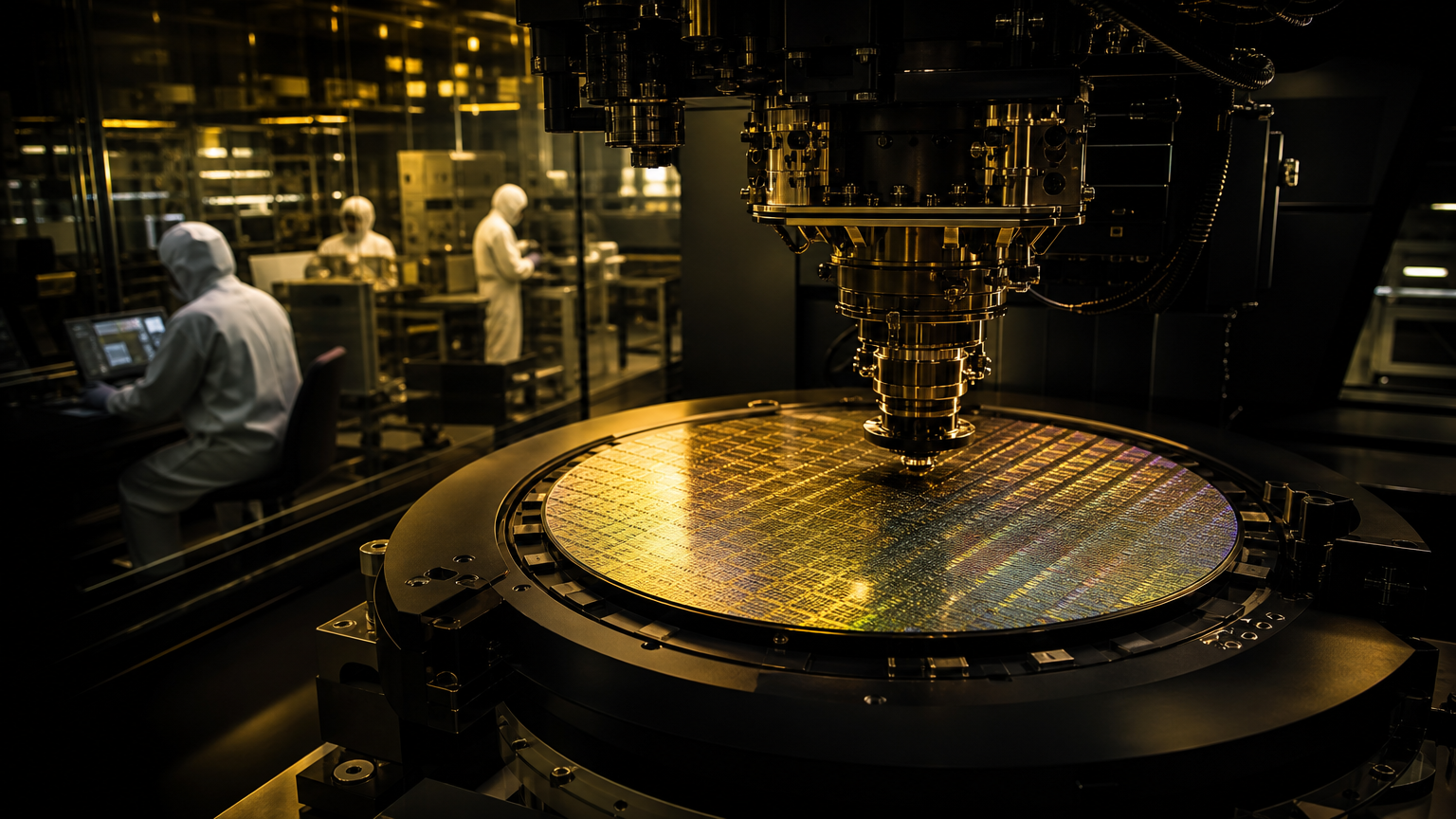
A $5 billion workshop for the next chip era
Applied Materials has officially unveiled its Equipment and Process Innovation and Commercialization Center, or EPIC Center, at its Sunnyvale, California campus, describing it as a $5 billion capital investment and the world’s largest facility dedicated to collaborative semiconductor process technology and manufacturing equipment R&D . The opening puts a large, highly visible stake in Silicon Valley at a moment when the chip industry is trying to squeeze more performance, better power efficiency and faster commercialization out of technologies that are becoming harder to scale .
The headline number matters, but so does the type of spending. This is not a conventional production fab designed to churn out commercial wafers. EPIC is a research and commercialization environment where Applied Materials says chipmakers, systems companies, equipment partners and university researchers will work alongside its own scientists and engineers . In practical terms, the company is trying to make the lab itself a shared platform.
The facility is massive by R&D standards: Applied says the building spans 600,000 square feet, contains nearly four acres of advanced cleanroom space and required more than six million construction hours to complete . SiliconANGLE reported that the center is meant to support parallel, cross-industry R&D under one roof, rather than the traditional model in which materials work, equipment development, process integration and pilot production are handled in separate stages .
Why Applied wants to change the R&D model
The strategic argument behind EPIC is simple: at advanced nodes, the old relay race is too slow. Applied describes the traditional development chain as a sequence of handoffs, with materials research, equipment development, process integration and pilot validation taking place in different environments . Each handoff can add delay, create mismatches and force engineers to rediscover problems later in the process.
At EPIC, Applied is trying to collapse those stages. The company says the center is designed to enable parallel rather than sequential development of materials, equipment and process technology, with the aim of shortening learning cycles and accelerating commercialization . TechTimes framed the opening as a shift away from “serial chip R&D” toward simultaneous co-development, particularly for the materials, equipment and processes required by AI-era chips .
That shift reflects a deeper industry reality. Leading-edge scaling is no longer just a story about shrinking transistors with better lithography. Applied and its partners are now pointing to a broader set of bottlenecks: new transistor structures, low-resistance wiring, advanced packaging, high-bandwidth memory, process control and hybrid integration . SiliconANGLE reported that projects inside the facility are expected to involve areas such as 3D architectures, advanced packaging, low-resistance wiring and hybrid bonding .
The partner roster is the real signal
The opening roster is unusually broad. Applied says EPIC begins with founding partners TSMC, Intel, Samsung Electronics, Micron and SK hynix; innovation partners Broadcom, Advantest, SCREEN, KIOXIA and Besi; and research partners Arizona State University, Rensselaer Polytechnic Institute, Stanford University, UC Berkeley and UCLA Samueli School of Engineering . That list spans foundry logic, integrated device manufacturing, memory, systems, test, equipment, packaging and academia.
The important point is not only that large companies are attached to the project. It is that some of them compete directly with one another, yet still have reasons to work close to the same toolmaker. Fortune reported that competing memory companies will have their own private test facilities inside the center, allowing them to work with Applied’s teams while protecting proprietary roadmaps . This is likely to become one of EPIC’s central tests: whether collaboration can be close enough to speed innovation without blurring competitive boundaries.
Applied’s logic is that earlier access to equipment and process options can help customers make better architecture decisions before a technology reaches the fab. Fortune reported that Applied expects the EPIC model to reduce the concept-to-commercialization timeframe for new chip architectures from a typical 10 to 12 years to as little as six years . SiliconANGLE separately cited Applied CEO Gary Dickerson as saying the center’s goal is to cut development cycle time by at least 30% .
Those claims should be read as targets, not guaranteed outcomes. Semiconductor history is full of promising process technologies that looked elegant in a lab and proved difficult in production. Still, the reason EPIC matters is that it tries to attack exactly that gap: the costly distance between a working idea and a high-yield manufacturing recipe.
AI demand turns R&D speed into a competitive weapon
The timing is not accidental. Applied presented the center as an answer to the demands of the AI era, where data-center accelerators, high-bandwidth memory and energy-efficient computing require rapid progress across multiple technology layers . At its SEMICON West investor breakfast one day later, Applied said AI infrastructure buildout is driving a new era of wafer-fab-equipment growth and that leading-edge foundry-logic, DRAM and advanced packaging are expected to drive around 75% of WFE growth from 2025 to 2030 .
That statement connects EPIC to a larger business thesis. Applied is not just opening a showcase lab; it is aligning its R&D footprint with the parts of the semiconductor equipment market it believes will grow fastest. The company said it plans to more than double its R&D lab and manufacturing capacity by 2030 and noted that it had announced 15 EPIC Center partnerships to date .
This is also why the facility’s location matters. Silicon Valley is no longer the center of global high-volume chip manufacturing, but it remains a dense node for chip design, semiconductor equipment, venture-backed hardware work and university research. Fortune described EPIC as a notable physical bet in a region better known today for software giants and low-slung campuses than for imposing semiconductor facilities . In that sense, the center is both industrial infrastructure and a statement about where Applied thinks the early stages of future chipmaking should be coordinated.
Beyond fabs: the new geography of semiconductor competition
For years, semiconductor policy and investment debates have focused heavily on fabs: where wafers are produced, how much capacity is domestic and which governments subsidize new plants. EPIC points to a complementary layer of competition. Before a process can be manufactured at scale, it has to be invented, integrated, tested, debugged and made repeatable. Applied is betting that the place where those steps happen will be strategically important.
That does not mean EPIC replaces fabs. It is better understood as an upstream accelerator for fabs. If successful, technologies developed there could arrive at customer factories with fewer unresolved integration issues, faster yield ramps and clearer equipment recipes. Applied says the center is intended to compress the timeline from early-stage materials research to high-volume manufacturing .
The most interesting consequence may be organizational rather than architectural. Semiconductor progress increasingly depends on co-optimizing many variables at once: materials, device structures, wiring, packaging, metrology, yield learning and system-level requirements. A facility that puts more of those decisions in the same building is a bet that coordination itself has become a technology.
What to watch next
The opening gives Applied a powerful narrative, but the proof will come later. The key questions are whether EPIC-generated processes reach customer fabs faster, whether partners deepen their work inside the center, and whether the model produces measurable gains in yield, cost, power efficiency or time-to-market. Applied’s own investor messaging makes clear that EPIC sits inside a broader plan to capture growth from AI-driven wafer-fab-equipment demand, services and advanced process leadership .
For now, the story is clear: Applied Materials has opened a $5 billion R&D hub meant to make semiconductor innovation less sequential, less fragmented and more collaborative . If the model works, the next big chip breakthroughs may not begin only in a fab. They may begin in a very expensive Silicon Valley workshop built to decide which materials, tools and process recipes are ready for the AI era.
Sources from the last 72 hours
- [1]Applied Materials Unveils $5 Billion EPIC Center in Silicon Valley to Accelerate Semiconductor Innovation for the AI EraOct 12, 2026, 10:30 PM
- [2]Applied Materials opens new $5B chip research facility to accelerate collaborative semiconductor innovationOct 13, 2026, 3:09 AM
- [3]Applied Materials Opens $5B EPIC Center, Replacing Serial Chip R&D With Parallel DevelopmentOct 14, 2026, 6:01 AM
- [4]Applied Materials Set to Outperform as AI Drives Sustained Demand for Wafer Fab EquipmentOct 13, 2026, 6:45 PM
- [5]Applied Materials’ $5 billion AI lab aims to cut chip development time in half—and restore Silicon Valley’s edgeOct 14, 2026, 1:15 AM
AI-generated article based on recent web research, then preserved as a dated editorial snapshot.
Comments
Be the first to comment.