
A groundbreaking that signals more than one fab
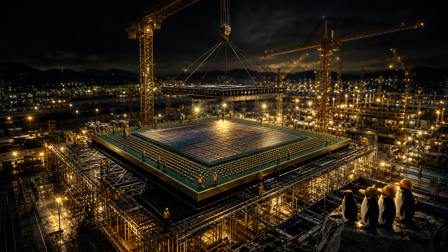
Samsung’s Chungcheong plan is no longer a slide in an investment briefing. On November 12, the group began construction at Samsung Electronics’ Onyang campus in Asan, South Chungcheong Province, formally starting a 144 trillion won regional buildout that brings together semiconductors, displays, package substrates and batteries . The ceremony was held at the future site of an advanced high-bandwidth memory packaging facility, with President Lee Jae Myung and Samsung Electronics Chairman Lee Jae-yong in attendance .
The headline number matters because this is not just a cleanroom expansion. Samsung’s announced total is split across four affiliates: 60 trillion won from Samsung Electronics, 67 trillion won from Samsung Display, 8 trillion won from Samsung Electro-Mechanics and 9 trillion won from Samsung SDI . Seoul Economic Daily reported that the plan is 4 trillion won larger than the 140 trillion won package announced in July, reflecting a faster and broader push to anchor core AI-era component production in Chungcheong .
At the center is Onyang Line 5, a new HBM-focused packaging line that Samsung Electronics wants operating by June 2028, one year earlier than initially planned . The line is designed as a three-story facility with about 31,000 square meters of cleanroom space, expanding the Onyang campus’s total floor area from roughly 270,000 square meters to 420,000 square meters once complete .
Why Onyang is becoming strategically important
Onyang has long been associated with assembly and test, but the new investment is meant to move it up the value chain. Yonhap reported that Lee Jae-yong described the site as transforming from conventional semiconductor assembly and testing into a major hub for advanced packaging, including HBM . That shift is significant because HBM is not only about making DRAM wafers; it is also about stacking, bonding, testing and packaging memory so it can feed data-hungry AI accelerators fast enough.
Samsung Electronics plans to invest 46 trillion won at Onyang to build five HBM production lines, including 6 trillion won for construction and 40 trillion won for advanced equipment deployed in phases . Within Samsung Electronics’ broader 60 trillion won Chungcheong commitment, Onyang and nearby Cheonan are being tied together as a production base for HBM and advanced back-end processing .
The timing shows where Samsung sees the bottleneck. Korea Times reported that Samsung is accelerating operations to meet rising demand for server memory and that, during its latest quarterly earnings discussion, the company said 2027 HBM supply negotiations had been completed while customers were still asking for additional volumes . In other words, the project is not only a long-range industrial-policy statement; it is also a response to near-term capacity pressure.
A regional cluster, not a single-company campus
The Chungcheong buildout is broader than Samsung Electronics. Samsung Display’s 67 trillion won investment will focus on Asan and Cheonan, including a new OLED line for foldable devices, laptops and tablets that is targeting mass production in the second half of 2029 . Samsung Electro-Mechanics is investing 8 trillion won in the region, including a Sejong expansion for flip-chip ball grid array substrates used in AI servers and high-performance computing, with mass production planned for September 2028 . Samsung SDI plans to invest 9 trillion won in Cheonan to strengthen next-generation battery development and production-process validation .
That mix is important. AI supply chains do not end at memory chips. They require advanced substrates, dense packaging, displays for new devices and batteries for increasingly power-aware systems. Samsung’s regional plan therefore looks less like a standalone fab and more like a concentrated components ecosystem.
The government is framing it the same way. KBS World reported that the Chungcheong groundbreaking is the first of three regional megaprojects tied to a combined 1.558 quadrillion won investment agenda across semiconductors, physical AI and AI data centers . Korea JoongAng Daily separately described the ceremony as part of a wider public-private push to build high-tech industry outside the Seoul metropolitan area, with the Chungcheong project moving from announcement to construction in about four months .
Jobs, permits and the politics of execution
The project’s scale also makes execution a political issue. The Onyang facility is expected to create about 700 direct jobs, while construction is projected to generate 2.6 trillion won in economic output and employ an average of 3,400 workers a day during the build period . President Lee used the ceremony to pledge support on permits, power, water and other infrastructure so that regional investments in Chungcheong, Honam and Yeongnam can proceed on schedule .
That emphasis on speed is not accidental. Financial News reported that the president told a public-private review meeting that what matters now is “execution, not promises,” and said six of eight anchor companies in the Chungcheong program had begun investments in earnest . The same report said 112 companies in sectors including semiconductors and biotechnology plan an additional 23.6 trillion won of investment in the region, beyond the 392 trillion won initially planned .
Samsung’s supplier base is also part of the story. Financial News reported that 194 partner companies connected to Samsung plan to invest about 18.1 trillion won in South Korea by 2030 . If that capital follows the anchor projects into materials, parts, equipment and specialized process services, the Chungcheong plan could become a multiplier rather than a set of isolated corporate facilities.
What it means for the global chip race
Samsung’s move comes as HBM has become one of the decisive battlegrounds in AI hardware. Advanced AI processors need memory that can deliver high bandwidth close to the compute engine, and HBM packaging is increasingly where performance, yield and capacity meet. Edaily noted that as HBM products move toward HBM4 and HBM4E, package complexity rises because data speed, power efficiency and heat dissipation have to be handled together .
That helps explain the size of Samsung’s bet. A company can design competitive memory, but without enough advanced packaging and test capacity, final HBM supply can still lag demand. By putting 46 trillion won into Onyang alone and building a five-line HBM base, Samsung is trying to remove one of the most expensive bottlenecks in the AI memory chain .
The buildout also reinforces Korea’s domestic supply strategy. The government wants leading companies to place strategic capacity in regional clusters, while Samsung wants to compete more aggressively in the AI memory cycle. Chungcheong now sits at the intersection of those goals: a place where national industrial policy, local economic development and Samsung’s HBM ambitions are being poured into concrete, cleanrooms and equipment orders.
The risk is that multiyear megaprojects can be slowed by power constraints, permitting, equipment lead times and market cycles. The opportunity is that if AI memory demand remains tight into 2028, Samsung could bring a much larger domestic HBM packaging base online just as customers are still chasing capacity. That is why this 144 trillion won buildout should be read as more than a regional construction plan. It is Samsung’s attempt to turn the AI boom into manufacturing depth at home, and Korea’s attempt to make the next chip race harder to dislodge.
Comments
Be the first to comment.